Laboratory of Advanced Materials and Devices
Laboratory of Advanced Materials and Devices (AMDeLab) was established after the merge of the Applied Physics Laboratory, Optical Characterization Laboratory, Thermal Analysis Laboratory, and Laboratory for Electrical/Magnetic Characterization and micro/nano devices design. The laboratory was created with a vision of a versatile research structure oriented on the physicochemical characterization and study of materials and devices. AMDeLab belongs to the Department of Physics, Faculty of Sciences in Aristotle University of Thessaloniki.
The research activities of AMDeLab are focused in the following fields:
- Growth and synthesis of advanced materials.
- Physicochemical characterization, study of materials and devices.
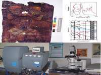
- Study of cultural heritage works.
The research plan of AMDeLab is developed in direct interaction to the needs of the production sector from local economy, taking advantage of the wide possibilities to offer integrated characterizations and studies of materials and devices together with its partnership in competitive research programs.
ΦΕΚ ίδρυσης: 4192/Β΄/27-12-2016
ΦΕΚ μετονομασίας (σε Εργαστήριο Προηγμένων Υλικών και Διατάξεων - AMDeLab): 3574/Β΄/26-9-2019
Telephone: +30 2310 998066
Email: Please turn on Javascript in your browser
Website: http://amdelab.physics.auth.gr/index-en.htm
DIRECTOR
George VourliasMEMBERS
- Konstantinos Chrissafis
- Eleni Pavlidou
- Dimitrios Tassis
- Evangelos Papaioanou
- Nikos Chastas
- Triantafillia Zorba
- Ioannis Samaras
RESEARCH ACTIVITY
Use of FTIR - UV/VIS in combination with thermal analysis methods to solve problems of technological materials
Α) High technology materials:
Narrow gap semiconductors, laminate compounds, γ and X-ray sensing materials, Sensors materials, Thermoelectric materials, Phase sensitive materials, Biodegradable polymers, Silicides, Phase sensitive materials, Optical data storage materials.
Β) Biomaterials:
Synthesis and Characterization of bioactive glass ceramics. Fabrication of composite materials with bioactive materials, Study of bioactivity in vitro, Cell-material interaction.
Γ) Cultural heritage materials:
Study and preservation of paintings and ceramics of cultural heritage.
Δ) Geological samples, (minerals, gemstones):
Mineral characterization, Classification of natural or artificial precious gemstones,Zeolithes, Oxides, Glass oxides, Glass waste materials.
The activities are held in collaboration with other institutes under the framework of national and international funding schemes.
RESEARCHERS
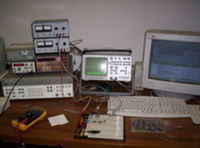
AC electrical measurements is an extension (in frequency domain) of the DC electrical measurements. AC electrical measurements may map the charges' transport (current) with common electrical elements (CEE) that we know from textbooks for DC/AC electrical circuits, i.e. we map the local charges' transport with CEE models. So, the parameters affecting current can be understood better, offering tools for material's optimization. For example, a piezoelectric quartz-crystal oscillator (PZT) has a simple direct model map between materials' or mechanical parameters of mass (m), spring constant (k) and energy losses (γ) with electrical equivalent model parameters of a coil (L), a capacitance (C) and a resistor(R) connected in series. This map is: m->L, k->1/C, γ->R. Thus, we may form a PZT-material's optimization process changing one (only) parameter in a well known RLC-model.
RESEARCHERS
 The activities of recent years in this research area consists of the development and study of physical properties of thick films, for the development of which several techniques are used. The research is performed in collaboration with the Department of Mechanical Engineering of the University. Several experienced researchers are involved along with PhD and postgraduate students.
RESEARCHERS
•Research Activities:
- Cognitive studies in Physics.
- Development of teaching activities (traditional and advanced technology).
- Development of integrated learning environments.
• Equipment:
1. Closed-loop TV circuit with capability of mixing sound and video in digital format (DVD), 4 SONY cameras, ZOOM 6x, video mixing console, U'matic video 3/4 250 lines.
2. Portable color video recorder JV-VHS 250 lines and video camera JVC KY-610, f = 1.4, ZOOM 10x.
3. Stereo color TV set (46").
4. Portable sound mixers (4 & 6 channels), directional and ambient microphones.
5. Devices for demonstration experiments in the fields of Mechanics, Electricity, Magnetism and Fluids.
6. Projectors for still and moving images.
7. A collection of videotapes VHS and DVD with experiments in Physics and a collection videotaped past student presentations.
8. Setups for on line measurements (MBL) and projection of educational activities.
RESEARCHERS
The electrical characterisation process aims to determine the electrical properties of materials and conductive systems as part of the general transport properties of solids. .
The group is specialised in the parametric study of the electrical behaviour of materials and its interpretation when exposed to controlled steady electric and magnetic fields. The parameters include temperature (10 – 300 K), magnetic field (1.4 T), the composition and structure of the materials, as well as the geometry and topography of the samples under test and their electrical contacts.
The characterisation process is based on the online measurement of the electrical conductivity, the Hall Effect and the magnetoresistance of materials, according to the Van der Pauw and Wascher methodologies. .
The group has extensive experience in the characterisation of semiconductors, metals and semi-metals, as well as in the exploration of suitable theoretical models in order to further investigate and expand the methodologies of measurement of inhomogeneous and anisotropic materials. .
RESEARCHERS
Research Activities:
•Thin Film Transistors of poly-nano-crystalline Si
•Nanoscale multigate MOSFETs •Nanomaterials, Quantum Dots in GaAs and Si
•Low Frequency Noise Characterization of Semiconductor Devices
•Hot Carriers Effects in CMOS Devices
•Theoretical Simulation of MOS Devices with the Silvaco Simulation Tool
•Compact drain current and low frequency Noise models in TFTs and nanoscale multigate MOSFETs
RESEARCHERS
A battery is an electrical source device offering charge, current and power for a load. High charge is offered using all volume (3D) of active materials. High current is offered by considerable mixed electronic-ionic conductivity of active materials (anode and cathode) as well as by high-ionic / low-electronic conductivity of the electrolyte during all working duty cycles of charge/discharge. So, a vast number of theoretical candidate materials for batteries, under the above constrains, is limited into an extemelly small number of materials for commercial batteries. The near future of batteries, though, is mainly the Li-ion Batteries, fulfilling better the consumers' demands for portable devices.
Activities:
A. Preparation of cathodic, anodic and electrolytic materials either in powders or in thin films
B. Investigation of the structural properties of these materials
C. Investigation of their electrical properties
D. Formation of Li-ion batteries and microbatteries
E.Investigation of the batteries by measuring the charging-discharging, the charge capacity and the stability of their properties with the number of cycles of charging-discharging.
RESEARCHERS
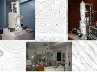
The Electron Microscopy Laboratory (EML) of Physics Department was established in 1963. The Lab is located at the west wing of the Science School and belongs to the Solid State Physics Section of the Physics Department. Today, the Lab comprises seven research staff members and two staff for technical support. The Lab hosts PhD and MSc Students, as well as Marie Curie Research fellows. The mission of EML is to provide to its members access to materials characterization equipment, training, and consultation, as well as to perform a range of services for end-users in the area of electron microscopy. In general, the laboratory’s activity comprises the integrated structural characterization and study of solid materials (metals, ceramics, polymers, glasses), as well as complex materials and composite crystals of advanced materials such as semiconductor thin films, nanostructures and heterostructures, natural or engineering materials in powder form and coatings. Μore specifically, the current research activity includes:
•Study and structural characterization of various materials (metals, semiconductors, ceramics, polymers, composites and advanced materials) by various transmission electron microscopy (TEM) techniques.
• Study of the nanostructure and structural defects of bulk materials, thin films and nanomaterials by High Resolution Transmission Electron Microscopy (HRTEM).
• Localized crystallographic and topological characterization of phases, interfaces, symmetries, orientation relationships, polarity, and line, planar or other extended structural defects.
• High accuracy nanoscale determination of internal strain fields.
• Structural and chemical characterization of homophase and heterophase interfaces down to the atomic scale.
• Integrated structural characterization of nano-heterostructures such as quantum wells, quantum dots, and nanowires.
• Study of nano-scale interaction mechanisms between defects, interfaces, internal fields and the kinetics of growth.
• Growth and characterization of engineering materials fabricated by advanced methods mechanosynthesis and thermal treatment.
• Study of phase transitions and vitrification of amorphous glassy materials.
• Research of transformation of phases and the crystallization of amorphous alloys by in situ thermal treatment.
• Development of integrated models of structures, interfaces and defects through the simulation of CTEM and HRTEM observations by computational methods such as Molecular Dynamics, ab initio DFT, and Monte-Carlo.
• Development of methods and software form quantitative HRTEM (qHRTEM) analysis (e.g. peak finding methods).
• Electron microscopy simulations of diffraction patterns, CTEM and HRTEM images. Software development for the processing and analysis of TEM images and diffraction patterns.
• Study of surface morphologies and properties by atomic force microscopy (AFM).
Through collaborations with international acknowledged electron microscopy centres:
- Two-dimensional nano-scale chemical mapping
- Chemical imaging of atomic structures.
- Nano-scale quantitative determination of chemical concentration.
- Nano-scale chemical profile determination across interfaces.
- Analysis of chemical bonding.
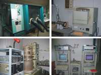
Instrumentation
The EM Laboratory possesses the necessary instrumentation for the precise HRTEM and CTEM characterisation of solid matter, as well as state-of-the-art instruments for TEM sample preparation, such as:
• High Resolution Transmission Electron Microscope JEOL 2011 (200KV), with a point resolution of 0.194 nm (purchased 2001). The microscope is equipped with:
i. KeenView G2 TEM CCD camera system (Olympus Soft Imaging Solutions)
ii. SPININGSTAR P020 device, for the precession and tilting of the electron beam (Nanomegas) accompanied with the necessary software.
• High Resolution Transmission Electron Microscope JEOL 2000FX (200KV), with a point resolution of 0.28 nm (purchased 1992).
• Conventional Transmission Electron Microscope JEOL 1010 (100KV) with a resolution 0.5nm, with heating, cooling and tensile stress facilities (purchased 1978).
• Atomic Force Microscope (AFM) Explorer 2000 Truemetrix Topometrix, with two scanners of (100X100) μm, (2.5X2.5) μm, and a liquid scanner of (2.5X2.5) μm. Resolution in the nanometre scale. Working at Contact mode, Tapping mode, Lateral Force mode.
• Argon ion-milling machines: Edwards (model IBMA2), MTA-MFKI and TECHNOORG LINDA with a liquid nitrogen facility.
• Precision ion polishing system, PIPS Gatan (model 691).
• Diamond lapping and polishing machine for use with the tripod polisher, South Bay Technology (model 910).
• Precise semi-automated grinding/polishing equipment, Allied MultiPrep.
• Precision dimpling instrument, South Bay Technology (model 515).
• Electropolishing devices Tenupol-2, Tenupol-3 (Struers).
• Dark room facility.
• Software for HRTEM image processing and simulations.
RESEARCHERS
The research activities of the Thermal Analysis lab are:
•Thermal characterization of materials in the temperature range –150 till 1750 oC. The studied materials cover a large are such as: semiconductors, magnetic materials, rocks, polymers, ceramics, biomaterials etc.
•Kinetic study of amorphous materials
•Kinetic study of phase transformation and decomposition
And specifically with:
•Thermal characterization of polymers - biocompatible polymers - nanocomposite polymers. Kinetic study of the crystallization of these materials. Study of thermal stability and kinetics of thermal degradation.
•Study of metal’s oxidation, coatings oxidation in high temperatures. Kinetic study of oxidation.
The equipments of the Thermal Analysis lab are:
1.Differential Scanning Calorimeter (DSC), SETARAM-DSC 141, which covers the temperature area –150 till 550 oC
2.Thermogravimetry (TGA), SETARAM SetSys 16/18 TG-DTA, which covers the temperature area 20 till 1750 oC