Optics and Spectroscopy Laboratory
The Optics and Spectroscopy Laboratory covers the educational and research needs of the Physics Department in the disciplines of Optics, Optical Signal Processing, Photonics and Spectroscopy in the Visible and the X-rays spectral regions. The Laboratory organizes and participates in public and private school training events on topics related to Optics and its Applications, while also participates at the annual "AUTH on Sunday" event of the Aristotle University of Thessaloniki.
DIRECTOR
Ioannis ArvanitidisMEMBERS
- Eleni Paloura
- Sotirios Ves
- Maria Katsikini
- Konstantinos Papagelis
- Maria Gioti
- Konstantinos Vyrsokinos
- Chrysoula Metaxa
- Fani Pinakidou
- Evaggelos Vanidis
- Eleni Vigka
- Nikolaos Vouroutzis
RESEARCH ACTIVITY
By using spectroscopic techniques (Raman, IR, absorption, Photoluminescence) and the synergy of theoretical calculations (phenomenological models, first-principles calculations, group theory) the optical properties of a wide range of materials (semiconductors, fullerenes, carbon nanotubes, garnets, low-dimensional materials etc.) are studied. These techniques and theoretical methods are utilized for materials characterization (identification of polytypes and phases, crystallinity, presence of mechanical stress/strain, chemical functionalization, electronic doping etc.) as well as for the study of fundamental physical phenomena (electron-phonon interaction, Kohn anomalies, immediate neighboring interactions etc.).
Moreover, the influence of external perturbations (temperature, uniaxial or biaxial mechanical deformation, hydrostatic pressure, electrochemical doping etc.) modifies drastically the optical properties of a material providing, thus, information on the physical phenomena themselves and allows the investigation of structural stability and the study of pressure induced structural or electronic phase transitions of materials.
- Indicative activities:
- Study of optical properties under normal conditions, high pressure and as a function of temperature of materials such as semiconductors (ΙΙΙ-V, II-VI), fullerenes and related compounds, chemically modified carbon nanotubes and scheelite compounds (ABO4, Α = Ca, Sr, Ba and B = W, Mo).
- Study of the optical properties of two-dimensional materials such as graphene (single or multilayers), BN, transition metal dichalcogenides (MoS2, WS2, Mo1-xWxS2, MoSe2) as a function of their interaction with various substrates, physical or chemical electronic doping, mechanical deformation and hydrostatic pressure.
- Study of III-V nitrides (AlN, Gan, InN and their alloys) using Raman spectroscopy: effect of ion implantation and doping as well as of the stresses induced during the epitaxial growth.
- Lattice dynamics of the rare earth aluminum and gallium garnets in a crystal form and as solid solutions (RE3Al5O12 and RE3Ga5O12, RE=rare earth).
- Equipment:
- Raman and photoluminescence set-up consisted of a triple monochromator (DILOR ΧΥ) with gratings of 1800 lines/mm and a CCD (EG&G 1433-C) liquid-nitrogen-cooled detector.
- Raman spectrometer RAMALOG 5 equipped with a Peltier-cooled photomultiplier tube with GaAs photocathode and a triple-monochromator that covers the wavelength range 12000 – 28000 cm-1 (8500-3500Å), fully automated and PC controlled.
- Two Ar+ Lasers of Spectra Physics 2W.
- One Kr Laser of Lexel 1.5 W.
- One cryostat accompanied by a diffusion pump of Cryogenic that works down to 20 K.
- Gas membrane driven diamond anvil cells, micro-tensiometers for the application of mechanical deformation (uniaxial, biaxial).
RESEARCHERS
The research activities of this group, (Lab for Thin Films- Nanosystems & Nanometrology- LTFN) involve:
- Development of Flexible and Printed Electronic Devices for Energy, Lighting, Medicine, etc Applications.
- Growth and study of nanomaterials and thin films on 2D and 3D substrates in high and ultra high vacuum environment with the use of Physical Vapor Deposition- PVD.
- Surface engineering of inorganic and organic materials with the use of ion bonds and plasma.
- Study of optical and electronic, structural and nanomechanical properties of thin films and bulk materials with state of the art techniques (such as Spectroscopic Ellipsometry, X ray diffraction and reflection, Atomic Force Microscopy and Nanoidentation).
- Development of in-situ and real-time optical monitoring methods of atomic processes and interactions that take place during films growth or surface modification and activation.
The scope of the above mentioned activities is the development of the research in basic level (understanding the growth mechanisms of the thin films and nanostructures, correlation of the structure of thin films and nanostructures with the optical- electronic- mechanical properties, computational methods and techniques) and also application level.
The applications include new advanced materials for microelectronics, flexible electronic devices, photovoltaics, barrier in gas nanocoatings for flexible packaging, hydrogen sensors and biosensors, coatings for medical implants and biocompatible materials etc.
RESEARCHERS
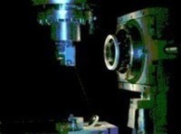
The Electron Microscopy Laboratory (EML) of Physics Department was established in 1963. The Lab is located at the west wing of the Science School and belongs to the Solid State Physics Section of the Physics Department. Today, the Lab comprises seven research staff members and two staff for technical support. The Lab hosts PhD and MSc Students, as well as Marie Curie Research fellows. The mission of EML is to provide to its members access to materials characterization equipment, training, and consultation, as well as to perform a range of services for end-users in the area of electron microscopy. In general, the laboratory’s activity comprises the integrated structural characterization and study of solid materials (metals, ceramics, polymers, glasses), as well as complex materials and composite crystals of advanced materials such as semiconductor thin films, nanostructures and heterostructures, natural or engineering materials in powder form and coatings. Μore specifically, the current research activity includes:
•Study and structural characterization of various materials (metals, semiconductors, ceramics, polymers, composites and advanced materials) by various transmission electron microscopy (TEM) techniques.
• Study of the nanostructure and structural defects of bulk materials, thin films and nanomaterials by High Resolution Transmission Electron Microscopy (HRTEM).
• Localized crystallographic and topological characterization of phases, interfaces, symmetries, orientation relationships, polarity, and line, planar or other extended structural defects.
• High accuracy nanoscale determination of internal strain fields.
• Structural and chemical characterization of homophase and heterophase interfaces down to the atomic scale.
• Integrated structural characterization of nano-heterostructures such as quantum wells, quantum dots, and nanowires.
• Study of nano-scale interaction mechanisms between defects, interfaces, internal fields and the kinetics of growth.
• Growth and characterization of engineering materials fabricated by advanced methods mechanosynthesis and thermal treatment.
• Study of phase transitions and vitrification of amorphous glassy materials.
• Research of transformation of phases and the crystallization of amorphous alloys by in situ thermal treatment.
• Development of integrated models of structures, interfaces and defects through the simulation of CTEM and HRTEM observations by computational methods such as Molecular Dynamics, ab initio DFT, and Monte-Carlo.
• Development of methods and software form quantitative HRTEM (qHRTEM) analysis (e.g. peak finding methods).
• Electron microscopy simulations of diffraction patterns, CTEM and HRTEM images. Software development for the processing and analysis of TEM images and diffraction patterns.
• Study of surface morphologies and properties by atomic force microscopy (AFM).
Through collaborations with international acknowledged electron microscopy centres:
- Two-dimensional nano-scale chemical mapping
- Chemical imaging of atomic structures.
- Nano-scale quantitative determination of chemical concentration.
- Nano-scale chemical profile determination across interfaces.
- Analysis of chemical bonding.
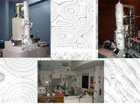
Instrumentation
The EM Laboratory possesses the necessary instrumentation for the precise HRTEM and CTEM characterisation of solid matter, as well as state-of-the-art instruments for TEM sample preparation, such as:
• High Resolution Transmission Electron Microscope JEOL 2011 (200KV), with a point resolution of 0.194 nm (purchased 2001). The microscope is equipped with:
i. KeenView G2 TEM CCD camera system (Olympus Soft Imaging Solutions)
ii. SPININGSTAR P020 device, for the precession and tilting of the electron beam (Nanomegas) accompanied with the necessary software.
• High Resolution Transmission Electron Microscope JEOL 2000FX (200KV), with a point resolution of 0.28 nm (purchased 1992).
• Conventional Transmission Electron Microscope JEOL 1010 (100KV) with a resolution 0.5nm, with heating, cooling and tensile stress facilities (purchased 1978).
• Atomic Force Microscope (AFM) Explorer 2000 Truemetrix Topometrix, with two scanners of (100X100) μm, (2.5X2.5) μm, and a liquid scanner of (2.5X2.5) μm. Resolution in the nanometre scale. Working at Contact mode, Tapping mode, Lateral Force mode.
• Argon ion-milling machines: Edwards (model IBMA2), MTA-MFKI and TECHNOORG LINDA with a liquid nitrogen facility.
• Precision ion polishing system, PIPS Gatan (model 691).
• Diamond lapping and polishing machine for use with the tripod polisher, South Bay Technology (model 910).
• Precise semi-automated grinding/polishing equipment, Allied MultiPrep.
• Precision dimpling instrument, South Bay Technology (model 515).
• Electropolishing devices Tenupol-2, Tenupol-3 (Struers).
• Dark room facility.
• Software for HRTEM image processing and simulations.
RESEARCHERS

1) "Speckle phenomena": Relating to the properties (statistically) of light (partial coherence and coherence) and the statistics of surfaces where the light is reflected or refracted. Our research is concerned with "Speckle" interferometry issues and optical image processing with carriers the "grains" of "Speckle".
2) Optical Image Processing: This is based on a general view of the scalar theory of diffraction of light in classical optics, which is called Furrier Optics. Our operations are mainly concerned with the research of methods of observing phase objects (e.g. transparent materials with variable refractive index).
3) Photorefractive Crystals: In these crystals phase gratings may be recorded. These phase gratings are carriers of record, storage and optical image processing. In specific sections of these crystals gratings are recorded versus the orientation of vector grating and versus the high voltage that is applied at their ends. With incidence in the grating of a proper light beam, the recorded information is reproduced via diffraction. We study the diffraction efficiency of gratings and the polarization properties of the diffracted beam, in terms of the polarization state of the incident beam, and other properties of phase gratings.
4) Physical Properties of Crystals: Here we are dealing with crystals which are: electro-optic, (Pockel effect), photo-elastic (via the inverse piezoelectric effect), optical-active, shows linear electro-gyration effect, etc. Using specified optical experimental arrangements we measure: The dispersion (depending on the wavelength) in the visible region of the electromagnetic spectrum: a) The refractive indices of crystals, b) The optical activity, c) The electro-optical coefficients and d) The electro-gyration coefficients.
5) Integrated Optics: In the course of the years past, integrated optics promised an exciting breakthrough through the development of photonic chips capable of controlling the light in a plethora of applications expanding from biological or chemical sensors and optical computing up to data communications. The research is actively operating in the area of integrated optics towards the development of integrated transceiver modules, photonic data interconnects and electro-optic switches, Quantum Random Generators and biosensor devices. Starting from the design, the research activities extend up to the complete characterization of active/passive integrated photonic components, i.e. carrier depletion modulators, plasmo-photonic modulators, grating couplers, multimode interference structures, ring-resonator based devices, routing elements, de/multiplexers and waveguide phase arrays, optical interfaces for active/passive devices in several material platforms and technologies.
6) Plasmonics: Plasmonics is a rapidly developing field that studies elementary polar excitations bound to metal surfaces. Plasmonic technology offer a new class of components with enhanced optical performance at ultra-small footprints below the diffraction limit. Current research efforts focus on bringing plasmonics in wafer scale CMOS lines to demonstrate low-cost fabrication of compact modules in the ever-growing areas of data communications and bio-sensing. The research is engaged in the simulation and characterization of integrated, on-chip, low energy electro-optic switches, ultra-sensitive biosensors and ultra-compact, ultra efficient, high speed modulators for data center interconnects.
7) Optical Phase Arrays: Optical phased arrays (OPAs) have recently drawn significant research attention due to their promising capabilities of non-inertial optical beam forming and steering delivering a variety of 3D sensing, imaging, illumination, ranging and optical wireless links. By manipulating the specific spatial distribution of the amplitudes and phases emitted from individual optical antennas, OPAs can form the desired radiation patterns through far-field interference. The research field is extended to the simulation of OPAs towards the development of compact and low power integrated beam steering devices for hybrid switching systems combining active waveguide and free space optics. In parallel there is strong experimental activity related to the characterization of OPAS assembled with cylindrical lenses for beam steering.
Laboratory Infrastructure
1. Optical and mechanical systems controlled by PC
2. Optical components and systems
3. Sources of Light and Lasers
4. Electronic Systems (oscilloscopes, power supplies, etc.)
5. Monochromators, spectrometers
6. Full range of microscopes
7. Diffractometers, interferometers and other optical instruments
RESEARCHERS
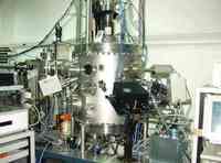
Study of the nanostructure (nearest neighbor distances, coordination numbers and bond angles) as well as optical properties (density of unoccupied states) in the soft and hard x-ray spectral region using x-ray absorption spectroscopies EXAFS & NEXAFS.
Elemental mapping using the x-ray fluorescence spectroscopy (XRF mapping) and micro XAFS. The samples under study are:
i) compounds of Si (mainly SiNx)
ii) group III nitrides (GaN, AlN, InN and their alloys)
iii) glasses and glass ceramics containing solid wastes (information on the sample preparation can be found in the web page of WFENV-NET http://web.auth.gr/wfenv-net
iv) biological samples for the determination of the trace element concentration
Moreover, inelastic X-ray (and alternatively neutron) scattering for the study of dispersion curves and the density of states of crystalline solids can be conducted.
The measurements are conducted at Synchrotron Radiation facilities:
BESSY http://www.hasylab.de,
HASYLAB http://www.bessy.de,
ELETTRA http://www.elettra.trieste.it,
ESRF http://www.esrf.fr.
RESEARCHERS
Activities:
- Dynamics and Kinetics of disordered solid state systems and fractals.
- Dynamics of neural networks and signal transfer.
- Estimation of electronic and optical properties of conventional and novel semiconductor material with technological applicability.
- Interface study (symmetry, energy and structure features) in polycrystalline materials with lattice model.
- Study of crystallite triplets in polycrystalline materials.
- Estimation of electronic and dynamic properties in crystals, amorphous materials, superlattices.
- Properties and Critical phenomena in ionic crystals.
- Lattice dynamics of crystalline solids (3D and 2D) using phenomenological models and first-principles calculations. Application of group theory for the interpretation of Raman and Infrared spectra.
- Difussion modelling, random walk, complex systems, low-dimensional systems, fractals, trapping events. - Statistical Physics Methodology.
Equipment:
PC Lab with parallel processing. Consists of 32 PCs (Intel Core 2 Duo, 64 processors), Total RAM 128 Gb, Storage Space 6.7 Tb, Operating System Scientific Linux.