Team MagnaCharta
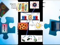
This group works on modern magnetic nanomaterials such as magnetic nanoparticles, multilayers and thin films. Our interests start from systematic synthesis and robust investigation of physical properties and conclude to technological applicability of nanomagnetism on diverse aspects such as information storage, biomedicine and sustainable growth.
DIRECTOR
Mavroeidis AngelakerisMEMBERS
RESEARCH ACTIVITY
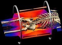
i. Diagnostic applications (electrical impedance tomography
ii. Therapeutic applications (microwave hyperthermia, RF ablation)
iii. Non-ionising radiation dosimetry (SAR assessment of telecommunications equipment).
RESEARCHERS
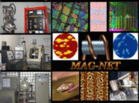
The group is involved in projects studying the phases, the microstructures and the morphology of magnetic materials focusing on correlations of structure and magnetism not only in bulk materials but in magnetic nanostructures as well. The various activities may be summarized as follows:
Α). Growth - Fabrication of magnetic materials of technological interest.
Β). Characterization and study of microstructure till the atomic level.
C). Temperature-dependent magnetic characterization.
D). Thermal, mechanical and magnetic treatments for improving the magnetic study.
E). Theoretical study and simulation of magnetic features.
•Equipment:
- UHV chamber with 3 sources for e-beam evaporation of thin and multilayered films.
- Monocrystal fabrication with Czochralski – Bridgeman method.
- Inductive furnace for metal casting and alloy formation.
- Vibrating Sample Magnetometer - VSM for thin films (77-300K, 0-1.2T, 0–2T).
- Moessbauer spectrometer 57Fe (77 – 300 K)
RESEARCHERS
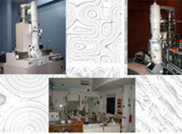
The Electron Microscopy Laboratory (EML) of Physics Department was established in 1963. The Lab is located at the west wing of the Science School and belongs to the Solid State Physics Section of the Physics Department. Today, the Lab comprises seven research staff members and two staff for technical support. The Lab hosts PhD and MSc Students, as well as Marie Curie Research fellows. The mission of EML is to provide to its members access to materials characterization equipment, training, and consultation, as well as to perform a range of services for end-users in the area of electron microscopy. In general, the laboratory’s activity comprises the integrated structural characterization and study of solid materials (metals, ceramics, polymers, glasses), as well as complex materials and composite crystals of advanced materials such as semiconductor thin films, nanostructures and heterostructures, natural or engineering materials in powder form and coatings. Μore specifically, the current research activity includes:
•Study and structural characterization of various materials (metals, semiconductors, ceramics, polymers, composites and advanced materials) by various transmission electron microscopy (TEM) techniques.
• Study of the nanostructure and structural defects of bulk materials, thin films and nanomaterials by High Resolution Transmission Electron Microscopy (HRTEM).
• Localized crystallographic and topological characterization of phases, interfaces, symmetries, orientation relationships, polarity, and line, planar or other extended structural defects.
• High accuracy nanoscale determination of internal strain fields.
• Structural and chemical characterization of homophase and heterophase interfaces down to the atomic scale.
• Integrated structural characterization of nano-heterostructures such as quantum wells, quantum dots, and nanowires.
• Study of nano-scale interaction mechanisms between defects, interfaces, internal fields and the kinetics of growth.
• Growth and characterization of engineering materials fabricated by advanced methods mechanosynthesis and thermal treatment.
• Study of phase transitions and vitrification of amorphous glassy materials.
• Research of transformation of phases and the crystallization of amorphous alloys by in situ thermal treatment.
• Development of integrated models of structures, interfaces and defects through the simulation of CTEM and HRTEM observations by computational methods such as Molecular Dynamics, ab initio DFT, and Monte-Carlo.
• Development of methods and software form quantitative HRTEM (qHRTEM) analysis (e.g. peak finding methods).
• Electron microscopy simulations of diffraction patterns, CTEM and HRTEM images. Software development for the processing and analysis of TEM images and diffraction patterns.
• Study of surface morphologies and properties by atomic force microscopy (AFM).
Through collaborations with international acknowledged electron microscopy centres:
- Two-dimensional nano-scale chemical mapping
- Chemical imaging of atomic structures.
- Nano-scale quantitative determination of chemical concentration.
- Nano-scale chemical profile determination across interfaces.
- Analysis of chemical bonding.
Instrumentation
The EM Laboratory possesses the necessary instrumentation for the precise HRTEM and CTEM characterisation of solid matter, as well as state-of-the-art instruments for TEM sample preparation, such as:
• High Resolution Transmission Electron Microscope JEOL 2011 (200KV), with a point resolution of 0.194 nm (purchased 2001). The microscope is equipped with:
i. KeenView G2 TEM CCD camera system (Olympus Soft Imaging Solutions)
ii. SPININGSTAR P020 device, for the precession and tilting of the electron beam (Nanomegas) accompanied with the necessary software.
• High Resolution Transmission Electron Microscope JEOL 2000FX (200KV), with a point resolution of 0.28 nm (purchased 1992).
• Conventional Transmission Electron Microscope JEOL 1010 (100KV) with a resolution 0.5nm, with heating, cooling and tensile stress facilities (purchased 1978).
• Atomic Force Microscope (AFM) Explorer 2000 Truemetrix Topometrix, with two scanners of (100X100) μm, (2.5X2.5) μm, and a liquid scanner of (2.5X2.5) μm. Resolution in the nanometre scale. Working at Contact mode, Tapping mode, Lateral Force mode.
• Argon ion-milling machines: Edwards (model IBMA2), MTA-MFKI and TECHNOORG LINDA with a liquid nitrogen facility.
• Precision ion polishing system, PIPS Gatan (model 691).
• Diamond lapping and polishing machine for use with the tripod polisher, South Bay Technology (model 910).
• Precise semi-automated grinding/polishing equipment, Allied MultiPrep.
• Precision dimpling instrument, South Bay Technology (model 515).
• Electropolishing devices Tenupol-2, Tenupol-3 (Struers).
• Dark room facility.
• Software for HRTEM image processing and simulations.
RESEARCHERS
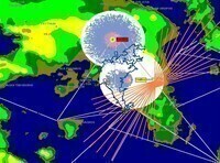
i. Coverage studies of telecommunication networks and broadcasting
ii. Assessment of emitted electric field from various devices
iii. Measurement and monitoring of the electromagnetic radiation in the environment
RESEARCHERS

Study of the nanostructure (nearest neighbor distances, coordination numbers and bond angles) as well as optical properties (density of unoccupied states) in the soft and hard x-ray spectral region using x-ray absorption spectroscopies EXAFS & NEXAFS.
Elemental mapping using the x-ray fluorescence spectroscopy (XRF mapping) and micro XAFS. The samples under study are:
i) compounds of Si (mainly SiNx)
ii) group III nitrides (GaN, AlN, InN and their alloys)
iii) glasses and glass ceramics containing solid wastes (information on the sample preparation can be found in the web page of WFENV-NET http://web.auth.gr/wfenv-net
iv) biological samples for the determination of the trace element concentration
Moreover, inelastic X-ray (and alternatively neutron) scattering for the study of dispersion curves and the density of states of crystalline solids can be conducted.
The measurements are conducted at Synchrotron Radiation facilities:
BESSY http://www.hasylab.de,
HASYLAB http://www.bessy.de,
ELETTRA http://www.elettra.trieste.it,
ESRF http://www.esrf.fr.
RESEARCHERS
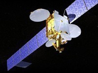
i. Telecommunications policy (broadband, advanced telecommunications services)
ii. Design and development of telecommunications networks (wireless and cable)
iii. Design of telecommunications systems components (antennas, transmission lines, filters, couplers, etc.)
iv. Telecommunications systems simulation
v. Development and analysis of telecommunications protocols
